MSI Super Q965 User Manual
Browse online or download User Manual for Motherboards MSI Super Q965. MSI Super Q965 User`s manual
- Page / 86
- Table of contents
- BOOKMARKS
- Intel® GME965 Chipset 1
- User’s Manual 1
- Revision History 2
- Preface iii 3
- Preface v 5
- Table of Contents 7
- List of Figures 9
- List of Tables 11
- 1 Introduction 13
- 1.2 Overview 14
- 1.3 Features 14
- 1.4 Specifications 15
- Power Consumption 17
- 1.5 Block Diagram 18
- 1.6 Functional Description 19
- Gigabit Ethernet 20
- PCI Express® 20
- Serial ATA II technology 20
- Hardware monitoring 21
- Watchdog Timer 21
- Software 21
- 1.7 Board Layout 22
- 1.8 Mechanical Drawings 23
- Dimensions in mm 24
- 2 Connectors & Jumpers 25
- Serial Port Connector (COM1) 26
- VGA Connector 26
- Audio I/O port 26
- USB Connectors 27
- LAN Port (RJ-45) 27
- 2.2 Onboard Connectors 28
- IDE Connector (IDE1) 29
- Digital IO Connector (J4) 30
- Front Panel Connector (JFP1) 31
- TV-Out Connector (JTV2) 32
- Serial Port Connector (COM2)) 34
- 2.3 Jumpers 35
- 24 Connectors & Jumpers 36
- 3 Getting Started 37
- 26 Getting Started 38
- Getting Started 27 39
- 3.3 Driver Installation 40
- 4 BIOS Setup 41
- Setup Menu 42
- Navigation 42
- BIOS Setup 31 43
- Hotkey Descriptions 44
- 4.2 Main Setup 45
- 4.3 Advanced BIOS Setup 46
- CPU Configuration 47
- IDE Configuration 47
- 36 BIOS Setup 48
- Super IO Configuration 49
- Hardware Health Configuration 50
- ACPI Settings 51
- APM Configuration 52
- Intel Robson Configuration 53
- MPS Configuration 53
- Trusted Computing 54
- USB Configuration 54
- 4.4 Boot Setup 55
- Boot Setting Configuration 56
- BIOS Setup 45 57
- Boot Device Priority 58
- Removable Drives 58
- 4.5 Security Setup 59
- 48 BIOS Setup 60
- 4.6 Chipset Setup 61
- North Bridge Configuration 62
- BIOS Setup 51 63
- South Bridge Configuration 64
- 4.7 Exit Menu 65
- Save Changes and Exit 66
- Discard Changes and Exit 66
- Discard Changes 66
- Load Optimal Defaults 66
- Load Failsafe Defaults 66
- BIOS Setup 55 67
- 56 BIOS Setup 68
- 5 POST Codes 69
- Appendix A - Watchdog Timer 73
- 62 Watchdog Timer 74
- Appendix B - System Resources 75
- SIO GPIO 76
- B.2 IO Map 78
- B.3 PCI Devices 79
- SMBus Resource Allocation 80
- ISA Interrupt Allocation 80
- ISA DMA Channel Allocation 81
- 70 System Resources 82
- Important Safety Instructions 83
- WARNING: 84
- Getting Service 85
- 74 Getting Service 86
Summary of Contents
Advance Technologies; Automate the World.Manual Rev.: 2.01Revision Date: December 12, 2008Part No: 50-1X002-1000MI-965Mini-ITX Industrial Motherboa
xList of FiguresThis page intentionally left blank.
List of Tables xiMI-965List of TablesTable 1-1: MI-965 General Specifications... 4Table 1-2: MI-965 Power Con
xii List of TablesThis page intentionally left blank.
Introduction 1MI-9651 IntroductionThis chapter will introduce the MI-965, its features, specificationsand applications. This chapter also provides de
2Introduction1.2 OverviewThe ADLINK MI-965 is a Mini-ITX industrial motherboard support-ing the next-generation Intel® Core 2 Duo/Intel® Celeron® pro-
Introduction 3MI-9651.4 SpecificationsSystemCPU/Cache • Intel® Core™2 Duo Mobile Processor T7500, 2.2GHz, 4MB L2 cache, 800MHz FSB• Mobile Intel® Cel
4IntroductionTable 1-1: MI-965 General SpecificationsI/O Interfaces (cont’d)Rear I/O • 2 RJ-45 LAN• 4 USB 2.0 ports• 1 D-Sub VGA connector• 1 serial
Introduction 5MI-965Power ConsumptionTable 1-2: MI-965 Power ConsumptionComponent DescriptionCPU Intel Core 2 Duo T7100 processorMemory Kingston 2G
6Introduction1.5 Block DiagramFigure 1-1: MI-965 Block DiagramSouthbridgeIntel® ICH8-MCPUIntel® Mobile Core™2 DuoCeleron®Socket P533/800MHz FSBNorthbr
Introduction 7MI-9651.6 Functional DescriptionProcessor SupportThe MI-965 motherboard features the Socket P interface designedfor Intel processors in
iiRevision HistoryRevision Release Date Description of Change(s)2.00 2008/10/02 Initial Release2.01 2008/12/12 Correct IO Shield Drawing
8Introductionhardware acceleration, 333 MHz display clock, and up to 384 MBof video memory, the Intel GMA X3100 provides a cost-effectiveand high-perf
Introduction 9MI-965Hardware monitoringA built-in, proactive hardware monitoring system in the ASIC mon-itors the CPU temperature, system fan rotatio
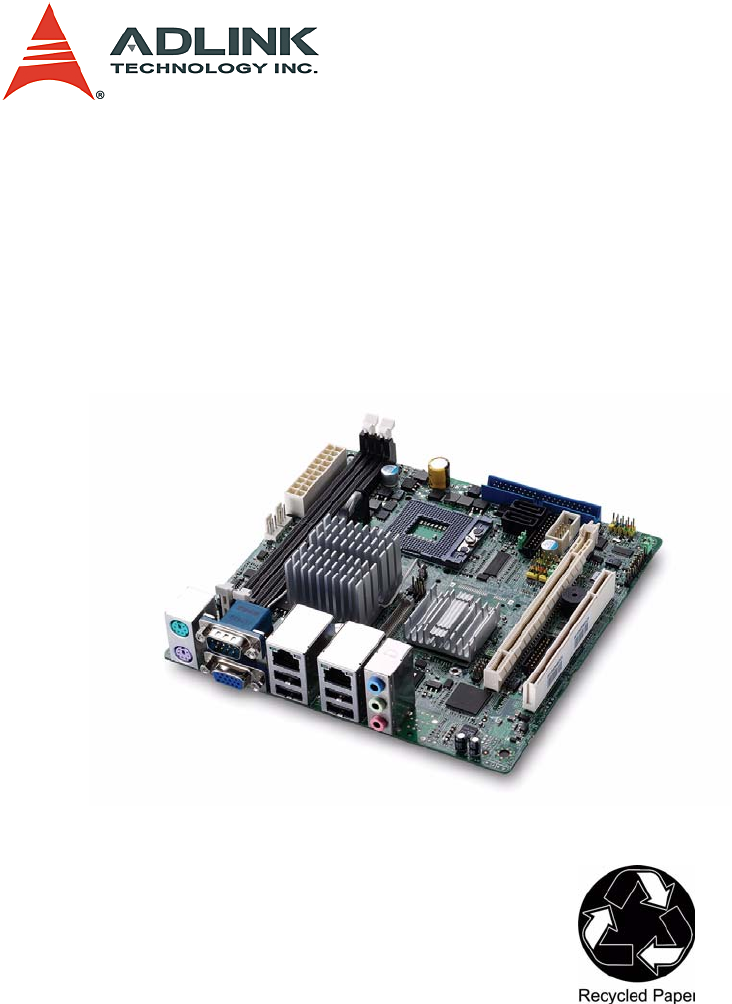
10 Introduction1.7 Board LayoutFigure 1-2: MI-965 Board LayoutJLVDS1DIMM1DIMM2JTV2JBAT1CPUFAN1SYSFAN1F_USB1F_USB2PCI1J4J7J6JCASE1J5JSPI2ALC888Intel825
Introduction 11MI-9651.8 Mechanical DrawingsFigure 1-3: MI-965 Board Dimensions (top view)Dimensions in mm
12 IntroductionFigure 1-4: MI-965 Rear I/O DimensionsDimensions in mm
Connectors & Jumpers 13MI-9652 Connectors & JumpersThe connectors and jumpers on the MI-965 allow you to connectand configure external device
14 Connectors & JumpersSerial Port Connector (COM1)VGA Connector.Audio I/O portThe three-jack audio I/O supports Line-In, Line-Out, and Mic-Infunc
Connectors & Jumpers 15MI-965USB ConnectorsLAN Port (RJ-45)This port allows gigabit connection to a Local Area Network (LAN)using a network hub.
16 Connectors & Jumpers2.2 Onboard ConnectorsATX Power Connector (ATX1)Chassis Intrusion Connector (JCASE1)This connector connects to the chassis
Connectors & Jumpers 17MI-965IDE Connector (IDE1)Pin # Signal Pin # Signal1 Reset IDE 2 Ground3 Host data 7 4 Host data 85 Host data 6 6 Host dat
Preface iiiMI-965PrefaceCopyright 2008 ADLINK Technology Inc.This document contains proprietary information protected by copy-right. All rights are r
18 Connectors & JumpersDigital IO Connector (J4)Serial ATA Connectors (SATA1-2))SPI Flash ROM Connector (JSPI2)Pin # Signal Pin # Signal1 VCC3 13
Connectors & Jumpers 19MI-965Fan Power Connectors (CPUFAN1, SYSFAN1)Front Panel Connector (JFP1)Pin # Signal Description1 HD_LED + Hard disk LED
20 Connectors & JumpersTV-Out Connector (JTV2)TV-Out Bracket (optional)Pin # Signal Pin # Signal1 GND 4 GND2 LCVBS 5 LC3 LY 6 NC
Connectors & Jumpers 21MI-965LVDS Flat Panel Connector (JLVDS1)Note: Refer to LVDS Power Selection Jumper (J7).USB Connector (F_USB1, F_USB2)Pin
22 Connectors & JumpersSerial Port Connector (COM2))Parallel Port Connector (JLPT1)Pin # Signal Functions1 DCD Data Carry Detect2 SIN Serial In or
Connectors & Jumpers 23MI-9652.3 JumpersLVDS Power Selection Jumper (J7)COM Port Power Jumpers (J5, J6)J5 corresponds to COM1, J6 corresponds to
24 Connectors & JumpersThis page intentionally left blank.
Getting Started 25MI-9653 Getting StartedThis chapter provides information on how to install components tothe MI-965 SBC. Specifically, the installat
26 Getting Started2. Carefully place the CPU into the CPU socket. Be sure toalign the gold triangle on the corner of the chip with thetriangular marki
Getting Started 27MI-9653.2 Memory Module InstallationThe MI-965 supports up to 4 GB of DDR2 533/667 SDRAM in two240-pin DIMM sockets. The DDR2 memor
iv PrefaceUsing this ManualAudience and ScopeThe MI-965 User’s Manual is intended for hardware techniciansand systems operators with knowledge of inst
28 Getting Started3.3 Driver InstallationThe MI-965 drivers are located in the following directories on theDriver CD, or can be downloaded from the AD
BIOS Setup 29MI-9654 BIOS SetupThe following chapter describes basic navigation for theAMIBIOS®8 BIOS setup utility.4.1 Starting the BIOSTo enter the
30 BIOS SetupSetup MenuThe main BIOS setup menu is the first screen that you can navi-gate. Each main BIOS setup menu option is described in thisuser’
BIOS Setup 31MI-965These keys include < F1 >, < F10 >, < Enter >, < ESC >, < Arrow >keys, and so on. .Note: There is a
32 BIOS SetupHotkey DescriptionsF1 The < F1 > key allows you to display the General Help screen.Press the < F1 > key to open the General H
BIOS Setup 33MI-965the < Enter > key to abort this function and return to the pre-vious screen.Enter The < Enter > key allows you to disp
34 BIOS Setupkeys to move between fields. The date must be entered in MM/DD/YY format. The time is entered in HH:MM:SS format.Note: The time is in 24
BIOS Setup 35MI-965CPU ConfigurationThis screen displays the advanced configurations of your CPU(non-configurable).IDE ConfigurationYou can use this
36 BIOS SetupATA/IDE ConfigurationThis item specifies whether the IDE channels should be initial-ized in Compatible or Enhanced mode of operation. The
BIOS Setup 37MI-965Super IO ConfigurationSerial Port 1 / 2 AddressSelect an address and a corresponding interrupt for Serial Port1/2.Parallel Port Ad
Preface vMI-965ConventionsTake note of the following conventions used throughout thismanual to make sure that users perform certain tasks andinstruct
38 BIOS SetupHardware Health ConfigurationThis option displays the current status of all of the monitored hard-ware devices / components such as volta
BIOS Setup 39MI-965ACPI SettingsSuspend ModeThis item specifies the power saving modes for ACPI function.If your operating system supports ACPI, you
40 BIOS SetupAPM ConfigurationPower Management/APMSetting to [Enabled] will activate an Advanced Power Manage-ment (APM) device to enhance Max Saving
BIOS Setup 41MI-965Intel Robson ConfigurationRobson is the code name for a new Intel platform technology thatuses non-volatile memory (Flash memory)
42 BIOS SetupTrusted ComputingThis setting controls the Trusted Platform Module (TPM) designedby the Trusted Computing Group (TCG). TPMs are special-p
BIOS Setup 43MI-965USB 2.0 Controller ModeThis setting specifies the operation mode of the onboard USB2.0 controller.Hotplug USB FDD SupportSet to [E
44 BIOS SetupBoot Setting ConfigurationQuick BootEnabling this setting will cause the BIOS power-on self testroutine to skip some of its tests during
BIOS Setup 45MI-965Bootup Num-LockThis setting is to set the Num Lock status when the system ispowered on. Setting to [On] will turn on the Num Lock
46 BIOS SetupBoot Device Priority1st Boot DeviceThe items allow you to set the sequence of boot devices whereBIOS attempts to load the disk operating
BIOS Setup 47MI-9654.5 Security SetupPassword SupportTwo Levels of Password ProtectionProvides both a Supervisor and a User password. If you useboth
vi PrefaceThis page intentionally left blank.
48 BIOS SetupRemember the PasswordKeep a record of the new password when the password ischanged. If you forget the password, you must erase the sys-te
BIOS Setup 49MI-965and press < Enter >. If the password confirmation is incorrect, anerror message appears. The password is stored in NVRAM aft
50 BIOS SetupNorth Bridge ConfigurationBoot Graphics Adapter PriorityThis item specifies which VGA card is your primary graphicsadapter.Internal Graph
BIOS Setup 51MI-965If you have a PCI Express X16 graphics card installed in yoursystem, you should disable this BIOS feature. This allows foroptimal
52 BIOS SetupBoot Display DeviceUse the field to select the type of device you want to use as thedisplay(s) of the system. Boot Display PreferencesThi
BIOS Setup 53MI-965GbE Wake Up From S5This field specifies whether the system will be awakened fromthe S5 power saving mode when activity or input si
54 BIOS SetupSave Changes and ExitWhen you have completed the system configuration changes,select this option to leave Setup and reboot the computer s
BIOS Setup 55MI-965designed for maximum system stability, but not maximum perfor-mance. Select the FailSafe Setup options if your computer isexperien
56 BIOS SetupThis page intentionally left blank.
POST Codes 57MI-9655 POST CodesThe POST code checkpoints are the largest set of checkpointsduring the BIOS pre-boot process. The following table desc
Table of Contents viiMI-965Table of ContentsMI-965... iRevision
58 POST CodesC6 Re-enable cache for boot strap processorC7 Early CPU Init Exit0A Initializes the 8042 compatible Key Board Controller.0B Detects the p
POST Codes 59MI-96540Detect different devices (Parallel ports, serial ports, and coprocessor in CPU, … etc.) successfully installed in the system and
60 POST CodesTable 5-1: POST Code CheckpointsAB Prepare BBS for Int 19 boot. Init MP tables.ACEnd of POST initialization of chipset registers. De-ini
Watchdog Timer 61MI-965Appendix A - Watchdog TimerThe following is a sample program for configuring the MI-965’swatchdog timer.A.1 Sample CodeSIO_IDX
62 Watchdog TimerThis page intentionally left blank.
System Resources 63MI-965Appendix B - System ResourcesB.1 Generic I/O PortsICH8M GPIOPin GPIO Typ Multi Power Connection. AG12 0 I/O BMBUSY#
64 System ResourcesTable B-1: ICH8M GPIO ResourcesSIO GPIOAF22 14 I/O EC_ME_ALERT 3.3v NC AG19 9 I/O WOL_EN 3.3v NC AG16 40 I/O OC1# 3.3v O
System Resources 65MI-965Table B-2: SIO GPIO Resources77 50 I/O WDTO#GP50 VSB GP502 23 I/O SCK/GP23 VCC NC88 34 O RSTOUT4#GP34 VSB NC69 36 I/O GP36
66 System ResourcesB.2 IO MapTable B-3: IO MapI/O Port Description0000-000F DMA Controller 10020-0021 Interrupt Controller 1002E-002F SIO Port0040-00
System Resources 67MI-965B.3 PCI DevicesTable B-4: PCI Device ResourcesPCI Interrupt Request RoutingTable B-5: PCI Interrupt Request RoutingPCI Dev
viii Table of Contents4 BIOS Setup ... 294.1 Starting the BIOS...
68 System ResourcesSMBus Resource AllocationTable B-6: SMBus Resource AllocationISA Interrupt AllocationTable B-7: ISA Interrupt AllocationDevice A
System Resources 69MI-965ISA DMA Channel AllocationTable B-8: ISA DMA Channel AllocationIRQ DescriptionCHANNEL0 Unassigned 8-bit channelCHANNEL1
70 System ResourcesThis page intentionally left blank.
Important Safety Instructions 71MI-965Important Safety InstructionsFor user safety, please read and follow all instructions,WARNINGS, CAUTIONS, and
72 Important Safety InstructionsX Never attempt to fix the equipment. Equipment should only be serviced by qualified personnel.A Lithium-type battery
Getting Service 73MI-965Getting ServiceContact us should you require any service or assistance.ADLINK Technology Inc. (Headquarters)Web Site: http://
74 Getting ServiceADLINK Technology Inc. (European Liaison Office)Sales & Service: [email protected] No.: +49-211-495-5552Fax No.: +49-
List of Figures ixMI-965List of FiguresFigure 1-1: MI-965 Block Diagram .............. 6Figure 1-2: MI-965 Boa
Related products and manuals for Motherboards MSI Super Q965
 (125 pages)
 (19 pages)
(28 pages)
(50 pages)
(66 pages)
(78 pages)
(19 pages)
(28 pages)
(50 pages)
(66 pages)
(78 pages)
 (21 pages)
 (152 pages)
(20 pages)
(81 pages)
(137 pages)
(152 pages)
(20 pages)
(81 pages)
(137 pages)
 (110 pages)
(130 pages)
(110 pages)
(130 pages)
© 2020, manymanuals.com. All rights reserved. | 0.194 s |
 Manymanuals.com
 Manymanuals.de
 Manymanuals.fr
 Manymanuals.it
 Manymanuals.pl
 Manymanuals.cz
 Manymanuals.es
 Manymanuals-pt.com
Comments to this Manuals